

Bose-Einstein condensation on an Atom Chip

Full size image |
On April 11, 2007, we obtained Bose-Einstein Condensation (BEC) for the first time on our Atom Chip. We are now working on optimizing it and preparing for experiments on the Atom Chip, concerning atom-surface interactions. We've recently started construction of a second BEC apparatus. |
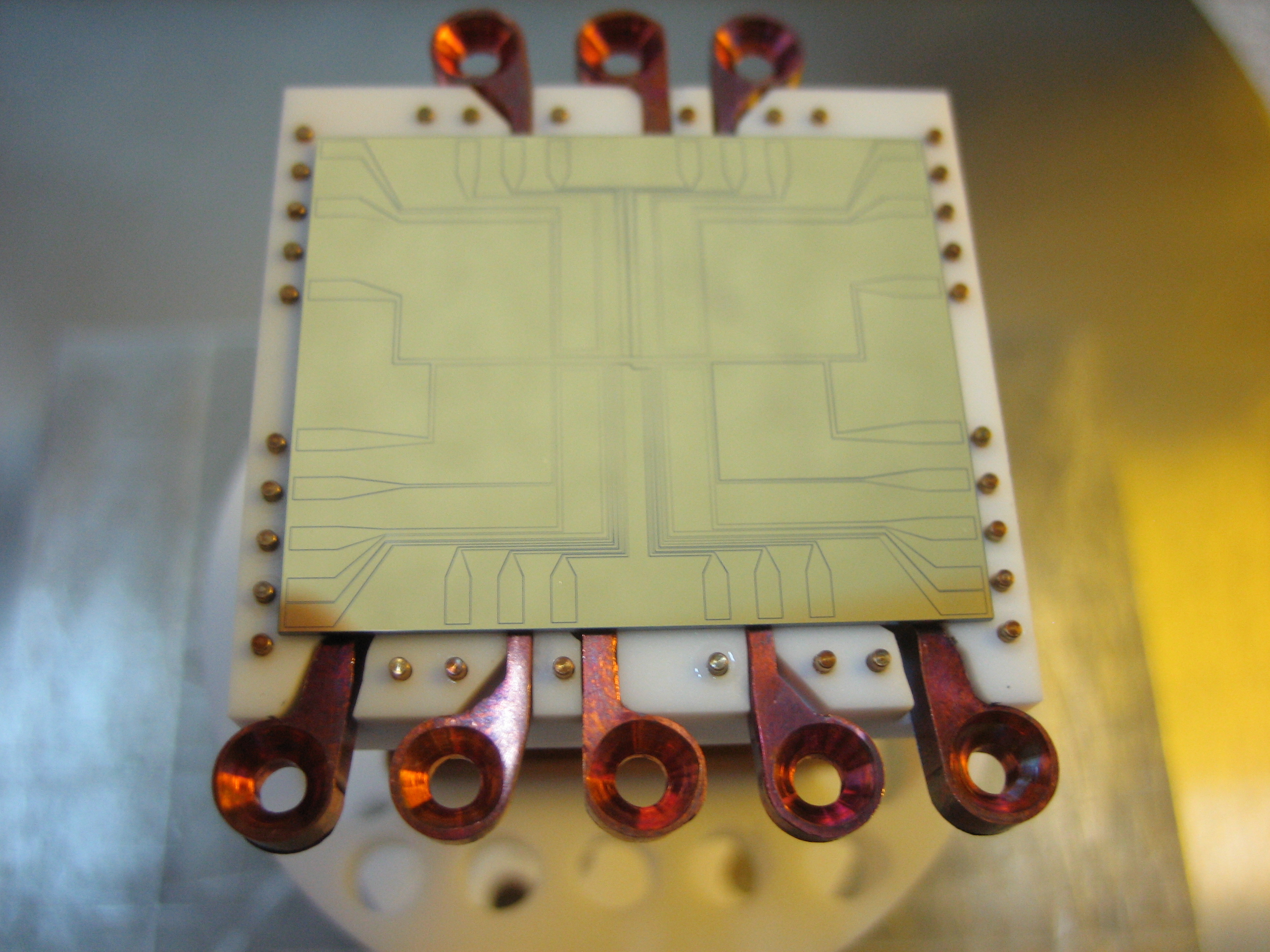
| The top picture shows our Atom Chip mounted before insertion into the experimental setup.
The chip is a Au-coated Si wafer, on which conducting wires are defined using lithography.
Beneath the chip there are a few large Cu structures used in the preliminary loading stages of the experiment.
Electrical contacts to the chip wires area made by bonding the small pins located around the chip to the Au surface (not shown).
Contacts to these pins, as well as to the Cu structures is made using UHV feed-throughs.
On the right, we show a series of images taken after releasing the condensate from its trap. The free expansion times (time-of-flight) are shown for each image. The width of the images is 207 µm, and the vertical distance between the images is scaled to represent the center-of-mass free fall of the atoms to gravity. The change in aspect ratio between the 2 axes of the cloud is one of the clear signatures of condensation. 
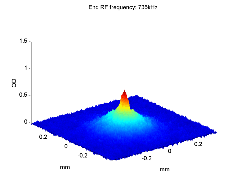
Finally, we show a series of images of the atoms cloud density profile from the onset of the transition to BEC at ~909kHz (corresponding to a trap bottom of ~1.3G), to a pure condensate. As the evaporative cooling final frequency is lowered below the transition point, the thermal component of the cloud gets smaller, until it is not noticeable at all anymore. In the intermediate stages, the bimodal momentum distribution is evident. |
Free Expansion
|