

Old projects
Carbon Nano-Tube Wire
Regular atom chips use gold for the wires that create the magnetic fields for the trap. These wires have many advantages, such as relatively high current density and easy and reliable fabrication. When the atoms are brought close to the wire, and the atom chip surface, some of the disadvantages start to appear.
For example, the fabrication of the wires is not perfect, hence, the wires are not perfectly smooth - they have some roughness at the edges. This roughness creates currents in different directions, which in turn create some corrugations in the atomic potential - instead of being smooth, the potential has hills and valleys. The atoms can "feel" the magnetic corrugations and they will behave accordingly, the atomic cloud will separate into different fragments.
Another disadvantage of the gold wires is the Johnson noise. This noise is created by the thermal energy of the electrons in the gold wire itself, regardless to the current in the wire. The fluctuating electrons create fluctuating magnetic fields which couple the magnetically trapped atoms to an un-trapped state. This coupling is expressed as atom loss and it is strengthen as the atoms are brought closer to the wire till at about 1µm height the atoms can not be trapped.
For these disadvantages the carbon nano-tube (CNT) should give an answer. It has many disadvantages on it's own, but it can give rise to new area of research. The main limitations of creating an atomic trap with a CNT are the random growth of the CNTs themselves and the limited absolute current (even though the current density is very high).
On the advantages side are the facts that there is no Johnson noise and that the current is smooth - no corrugations in the potential, hence the atoms can be trapped closer than 1µm from the CNT and the surface. At this distance the attractive Casimir-Polder force is important and it alters the atomic potential drastically.
The above imply that the atoms can be used to measure the Casimir-Polder force, or to measure atom-CNT interaction.
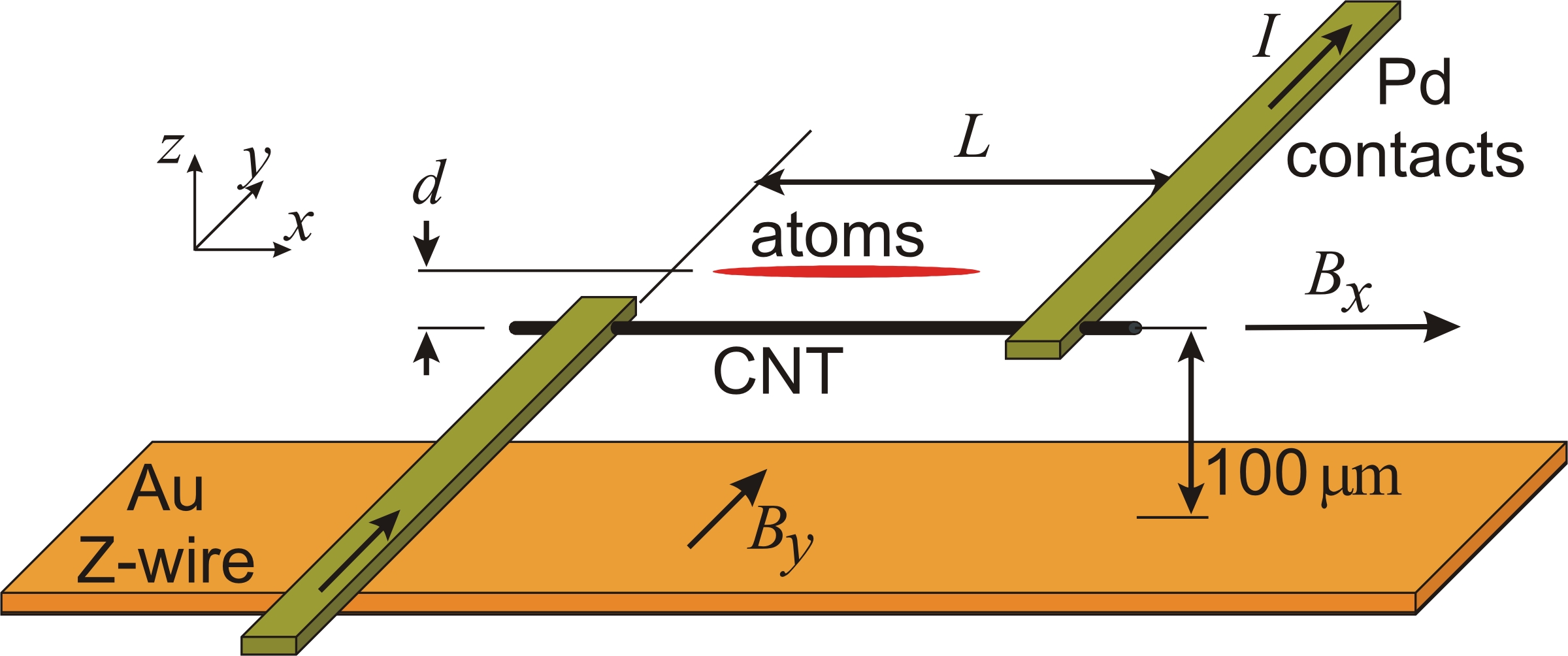
In this study, which has been published (see Papers, "Trapping cold atoms using surface-grown carbon nanotubes"), we check the possibility of trapping an atomic cloud with a "Z"-shaped trap where the center of the "Z" is made of a single layer CNT.
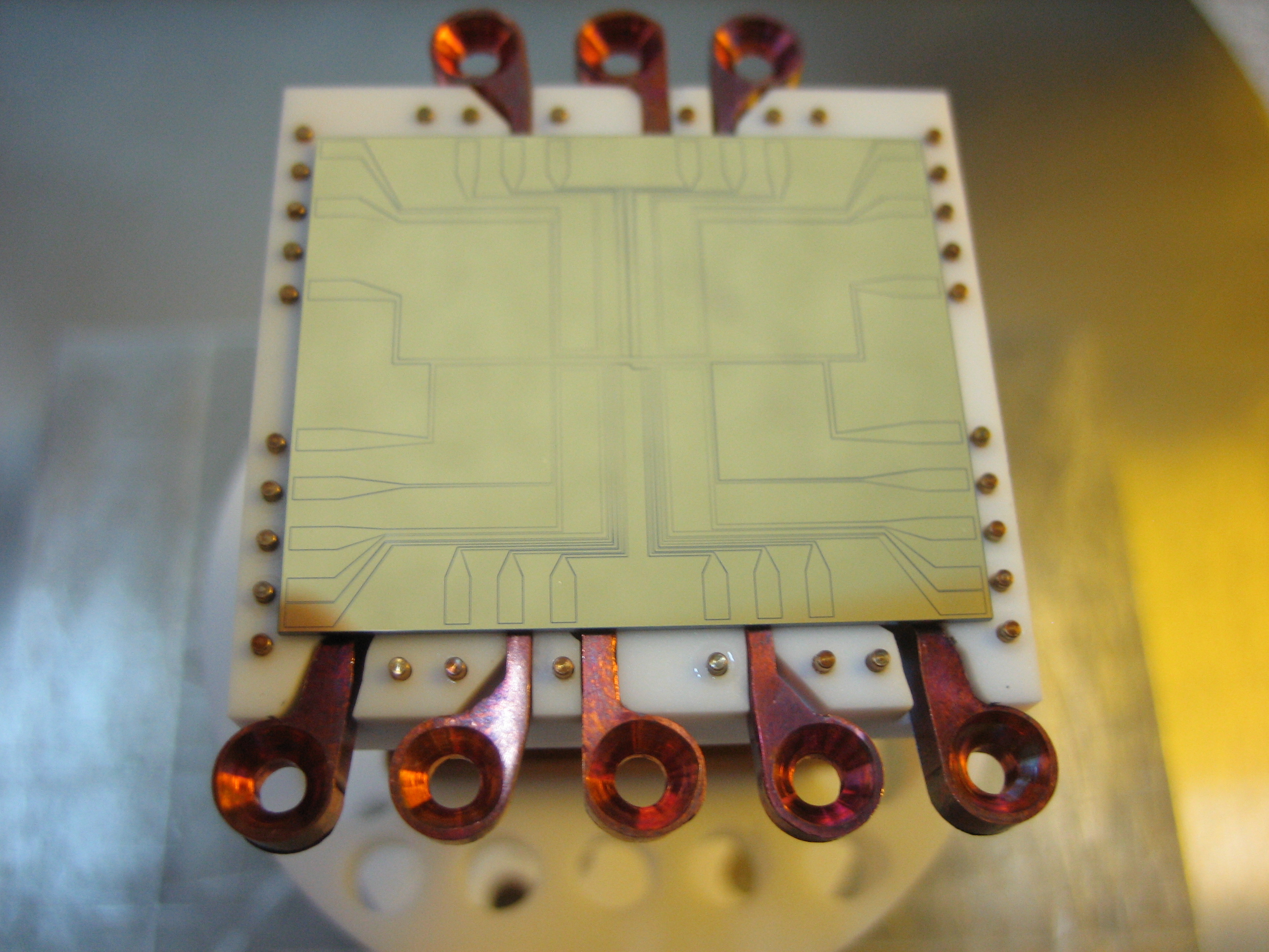
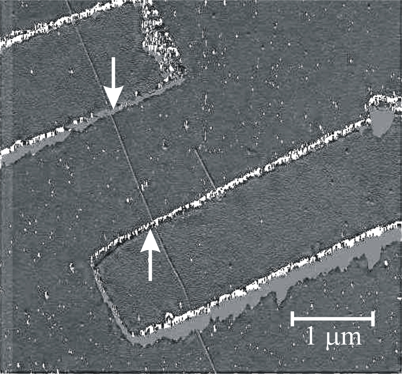
Below is shown a schematic representation of the two-layer CNT (left) and an atomic force microscope (AFM) image of a CNT fabricated and contacted for use as a "Z"-shaped wire trap for atom chip experiments (right). The CNT is marked with two arrows,and the macroscopic object are the Pd contacts.

Full size image |
 image of a CNT")
Full size image |
The atomic potential at the center of the atom chip is plotted on the image below (left), for three different trap positions. The total potential is the sum of the magnetic potential created by the current in the CNT and external fields, the gravity and the Casimir-Polder which bends all the curves to -∞ as they approach the surface. On the right, the barriers to the gravity and to the surface (CP) are plotted against the trap bottom position, together with the number of atoms each trap can hold.
 Full size image |
 image of a CNT") Full size image |
Anisotropic Materials
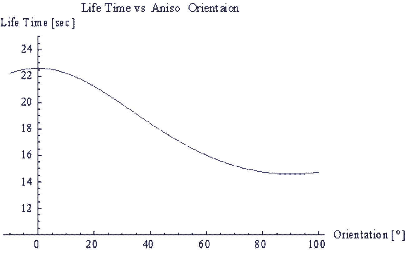
Close to a surface, the main source of atom loss is surface noise-induced spin-flips. If the surface is made from an electrically anisotropic material, the components of the magnetic-field's noise power spectrum change differently depending on the direction of the anisotropic material axes. By selecting a good conductivity axis of the anisotropic material in the direction of the Ioffe-Pritchard (IP) field of the magnetic trap (i.e. the direction of the atoms' polarization) and bad conductivity axes in the perpendicular directions we make one of the perpendicular components of the magnetic field's noise lower, causing a lower loss rate (the spin-flips loss rate depends on the perpendicular components of the noise spectrum). Rotating the material by 90 degrees will put the good conductivity axis in a direction perpendicular to the IP field making the perpendicular component of the magnetic field's noise higher and causing a higher loss rate.
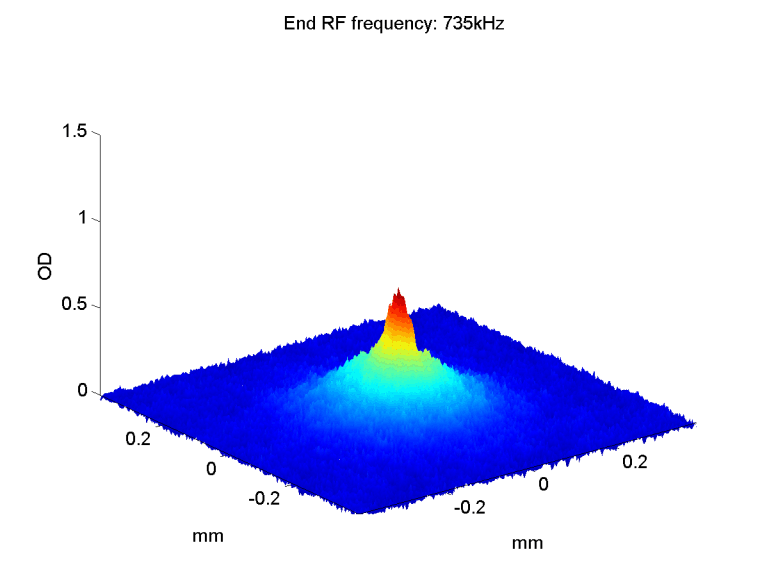
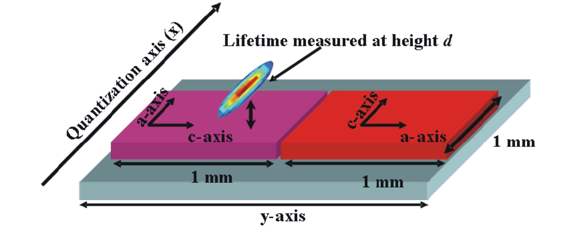
In our experiment we plan to place 4 pieces of a highly anisotropic material on an atom chip. Each piece will be put with its good conductivity axis at a different angle with respect to the IP field of our trap. The expected dependence of the cloud's life time on the orientation of the anisotropic material is shown in the graph below (left). On the right side an illustrative image of the cold atomic cloud above two anisotropic materials on an atom chip is shown.

Full size image |

Full size image |
For more information see "Magnetic interactions of cold atoms with anisotropic conductors" in Papers, and Tal David Thesis.