

Research
Introduction:
The high magnetic gradient generated by running currents in microstructures at the surface of an atomchip give the oportunity to generate very anisotropic traps and to rise new type of interesting regime. We have engineered a novel type of microstructure which use the extreme sensitivity of the atoms to directional deviations of the current in the wire to generate a 1D magnetic lattice. In this configuration the atomic clouds will be trapped in separated 1D traps.
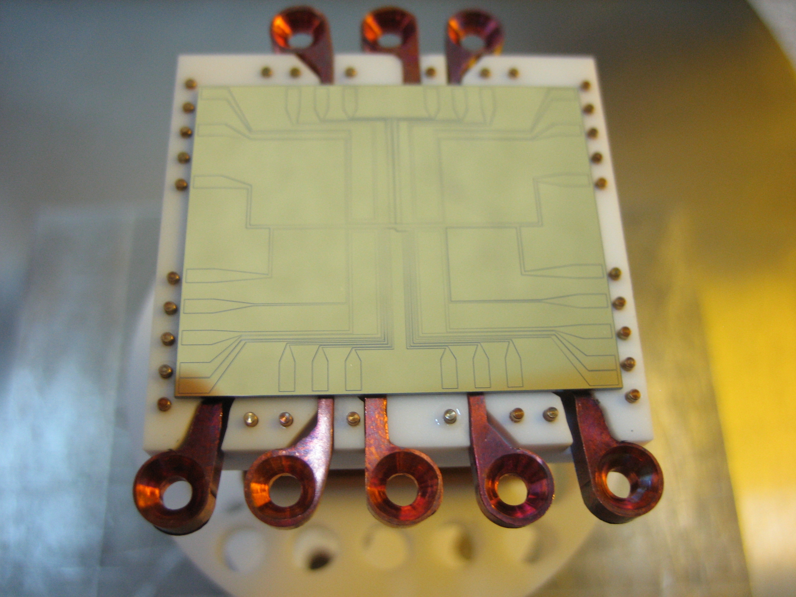
Our Atom Chip:
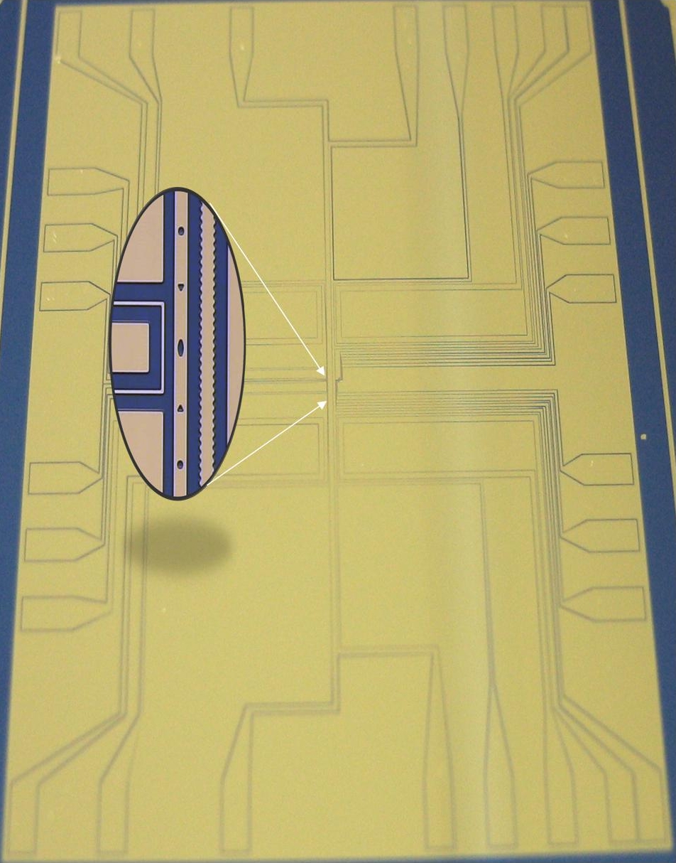
Left: The Atom Chip with all its gold wires. Right: The snake wire.
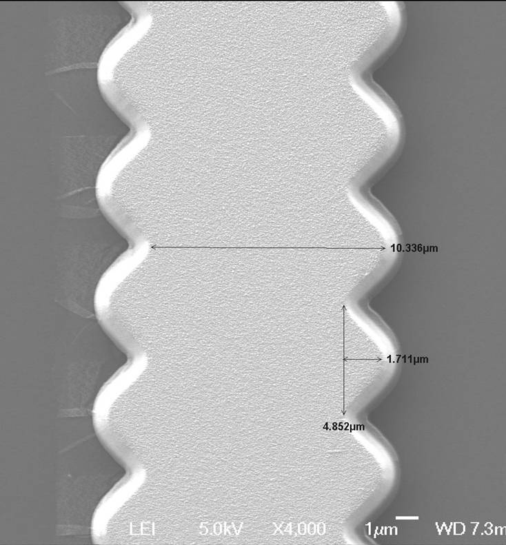
Directional deviation in the trapping wire current influences the trap minimum [See our paper: Aigner et al., Science 2008]. To generate a tunable 1D magnetic lattice, we have fabricated a wire with 5µm periodicity along the edges (see picture above). The lattice potential is exponentially dependent on the wire-atom separation d: most evident for d < 5 µm, and practically negligible for d > 20 µm.

Exemple of the isopotential (at 1µK) generated by the snake wire.
For different trap heights d, we can achieve different tunneling frequencies (Josephson tunneling). Typical trapping site frequencies have an aspect ratio of 1:20, this gives us a 1D BEC.
Our goal (expected results):
Once released from the magnetic lattice, the clouds expand and overlap. An interference pattern is formed. From the interference pattern one can extract information on the relative quantum phase between the separated clouds.
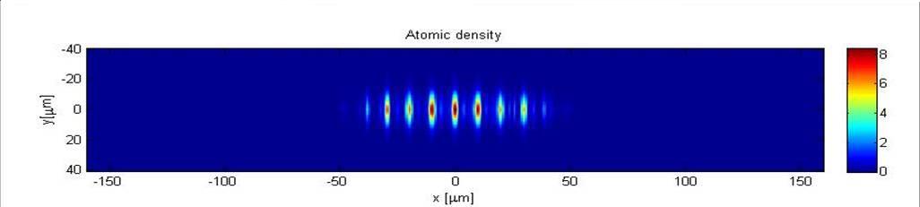
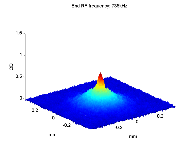
Exemple of interferences pattern once the clouds are released from the snake wire